A phone that costs $12. Image from (Huang, 2013)
Imagine you could buy a fully functional cellphone for $12. Such a device does actually exist, and while it might not include as many features as the latest iPhone, it does work, being able to make phone calls, play MP3 files, and send text messages. Most of the phone’s ‘smarts’ are in an integrated circuit, or IC, designed by the Taiwanese company MediaTek. As electrical engineering researcher and hacker Andrew Huang describes, this IC works as the phone’s brain, handling almost everything that the phone does, such as connecting to a mobile carrier’s network, making calls, texts, responding to button presses, and showing text on the screen. Despite all of its features, the IC by itself only costs about $2 (Huang, 2013). This phone isn’t the only device that uses ICs; in fact, almost every electronic device relies on one.
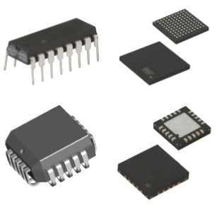
Some common IC packages. Image from (Strutz, 2015)
An IC comes in a package. As firmware engineer Shannon Strutz notes, these packages include leads—the metal pieces on the sides — which serve as the inputs and outputs of the IC. For example, in an IC used in a calculator, some leads might connect to the buttons, screen, or batteries. Each package involves different tradeoffs — some might be super small, but difficult to work with, while other packages might be larger but easier to use when you are manufacturing a product. Inside a package is the die (plural: dice), the part that ‘thinks,’ connected to the package’s leads with very thin wires (Ramsey, 2019). Made of silicon, the die contains hundreds of thousands of transistors used to make the IC actually do something (Ramsey, 2019). A transistor is like a light switch—it can either allow electricity to pass through or block it. You can create complex devices by connecting large numbers of transistors together.
The Design Process

Designing a die is like designing the floor plan of a house. Image of die from (Shirriff, 2016)
A major challenge is that someone needs to design the die. Shown above is a high-resolution scan of the die for a timer IC, taken by computer engineer Ken Shirriff (Shirriff, 2016), which might be used in a device like a flashing bike light. You can think of the process of designing a die to be like drafting the floor plan of a house. You might have only a certain amount of space to work with, and maybe you can’t move the ‘doors’ (inputs/outputs), but you can move things around in the space you have. Historically, dice were designed by hand, with engineers carefully cutting and placing tape to create the mask, which acts as the template for the die (Volk, 2001).

The mask is the negative of the die. Image modified from (Mack, 2019)
This mask is like the photo negative of the die—it gets projected onto the die, and whatever space isn’t blocked off by the mask is marked on the silicon (Mack, 2019). As technology improved, this mask design process quickly became computerized; however, it still remains one of the most important parts of the process.
It might initially seem strange that this process is so important; however, incredible amounts of effort go into these designs, as a well-designed IC can become quite popular. Consider the Z80, an IC released by a company called Zilog around 1976 (IEEE Spectrum, 2017). The Z80 was a processor—like the IC in the $12 phone—used in everything from cash registers to graphing calculators and game consoles (IEEE Spectrum, 2017). It was incredibly successful when first released, thanks in part to the fact that it was designed so that it was very easy to build a product with (Slater et al., 2007). Designers of the Z80 knew that their IC would be popular, and so they added ‘traps’ to their die—fake transistors unconnected to anything, but placed in strategic locations to seem important (Slater et al., 2007). That way, if someone were looking at the transistors on the die, trying to figure out how the IC worked, they would probably get confused (Slater et al., 2007). The traps seem to have actually worked, delaying a competitor’s clone of the Z80 by about 6 months (Slater et al., 2007).

A silicon wafer, ready for dicing. Image from (Miranda, 2010)
Once the die is designed, it must be manufactured. Dice are first manufactured on a silicon wafer (Miranda, 2010). The design is transferred onto these wafers, and then the dice are cut out of the wafer in a process known as dicing (Miranda, 2010). The exact manufacturing processes are complex, and most companies are secretive about the specific details of their processes. One of the most important traits of a process is called the minimum feature size, which specifies how small the structures on the die can be made. The timer IC from before, first produced in 1971, had a feature size of 16000 nanometers (nm), about twice the width of spider silk (Ramel, 2003; Scott, 2006). Modern ICs, such as what you might find in your smartphone or laptop, can have minimum feature sizes as small as 7 nm, 2000 times smaller than that used in the timer IC (Shankland, 2018).
Smaller and Smaller
Significant effort is put into developing processes with lower and lower minimum feature sizes.
Significant effort is put into developing processes with lower and lower minimum feature sizes. In fact, only two companies in the world are currently capable of manufacturing 7 nm devices: Taiwan Semiconductor Manufacturing Company (TSMC), and South Korean corporation Samsung (Merritt, 2018). Notably, in the U.S, Intel has struggled to move past 14 nm, with plans to manufacture smaller transistors running into several years of delays (Shilov, 2019).
Why is it so important to keep making this size smaller and smaller? It turns out that are many benefits related to a small feature size, but a major asset is that smaller transistors require a lot less power to operate (Kumawat, 2019). More specifically, if you have two dice with the same layout, but one has half the feature size, it will require roughly one fourth of the power (Kumawat, 2019). Imagine if your phone could last four times as long! In addition, making the transistors smaller means that you can pack more stuff into the same amount of space, so if you’re making an IC for a device where size is important (like a smartphone), you are able to produce something with more advanced features. This rapid improvement process, brought about by just making things smaller, is referred to as scaling (Kumawat, 2019).
This importance of scaling was recognized early on. In 1965, Gordon Moore, co-founder of Intel, predicted that about every two years, the number of transistors that could fit on a die would double, in what became known as Moore’s Law (Loeffler, 2018). Moore’s Law was treated as almost a challenge by the integrated circuit industry and has been closely followed for several decades (Loeffler, 2018). However, some believe that we reached the end of Moore’s Law around 2010, with many obstacles meaning that progress slowed down significantly (Dormehl, 2018).
A Leaky Faucet
At very small sizes, transistors act less like a perfect light switch, which is either on or off, and more like a faucet that’s being gradually turned on or off.
One of the biggest challenges with scaling is known as leakage current (Loeffler, 2018). At very small sizes, transistors act less like a perfect light switch, which is either on or off, and more like a faucet that’s being gradually turned on or off. As transistors become smaller, these ‘faucets’ aren’t able to turn off completely, meaning that some current ‘leaks’ through. In the best case, this current is just wasted as heat, making the IC less efficient; in the worst case, this current can go places that the IC’s designers never intended it to and wreak havoc. While historically this problem could be ignored, leakage current is a large headache in modern processes, and makes designing the die significantly harder (Loeffler, 2018). Imagine trying to build a house that conserved water, but all your faucets were always stuck half open.
While it makes the design process difficult, leakage current is relatively well understood and can be measured and accounted for. A more significant challenge relates to the lithography process mentioned earlier—that’s when the mask designed by the engineers gets projected onto the silicon. While it’s not too difficult to make a mask with small transistors on it, the projection process is the main issue (Bright, 2016). Currently, this projection process uses light with a wavelength of 193 nm (Moore, 2018). When the designs on the mask become smaller than that wavelength, the light is simply too big to fit through the cutouts on the mask (Moore, 2018). The current solution is to make multiple masks and offset them slightly, so that what ends up getting projected onto the silicon is the right size. However, this becomes tricky because the masks must be perfectly aligned (Moore, 2018). Additionally, to make transistors 5 nm and smaller, you would need over 100 masks, all of which must be precisely aligned (Moore, 2018), which isn’t really feasible.
One possible solution to this problem is a technique known as extreme ultraviolet lithography (Moore, 2018). EUV uses special ultraviolet light with a wavelength of 13.5 nm, which would easily fit through tiny gaps on the mask (Moore, 2018). The problem with this light is that it is very hard to work with (Bright, 2013). Specifically, it is almost impossible to use lenses with this type of light, because most lens materials just absorb the light entirely (Bright, 2013). This means that current equipment must be completely redesigned (Bright, 2013). In addition, due to the small wavelength, it requires a lot of energy to produce this light in the first place (Bright, 2013). One manufacturer of EUV equipment estimated the efficiency of their light source to be 0.02%, meaning that to get a bright enough light to be useful, you would need large amounts of power, which can get quite expensive (Kim, 2009).
It’s as if you had a miniature paintbrush and used it to paint whatever you wanted directly on the die, without needing a mask or any fancy light sources.
However, EUV is not the only potential solution. Some companies are looking into electron beam lithography or e-beam (Courtland, 2012). E-beam technology involves building a machine that fires a beam of electrons at silicon and using that to draw the IC design (Courtland, 2012). It’s as if you had a miniature paintbrush and used it to paint whatever you wanted directly on the die, without needing a mask or any fancy light sources. This technology makes it easy to create very small transistors all the way down to a size of about 2 nm (Manfrinato, 2013; Berggren, 2019). The main downside of this technology is its very slow speed—about 10 million times slower than the current state-of-the-art, taking days or even weeks for a single IC. The main issue is that, at smaller sizes, the movements of the electron beam must slow down significantly (Berggren, 2019; Courtland, 2012). Again, it’s like a paintbrush—making broad, large strokes is easy, but creating tiny, precise designs requires a smaller brush and more careful work. Intensive research is being conducted in ways to speed up this process, with two main solutions: using multiple beams at once (adding additional painters) or improving the accuracy of the beam (using better quality brushes) (Berggren, 2019; Courtland, 2012; Manfrinato, 2013; Manfrinato, 2015).
In addition, another solution being explored involves using a different material. With transistors of a size around 2 or 3 nm, you eventually run into fundamental limits of silicon, where each transistor uses only 10 atoms, and it is physically impossible to make things smaller (Waldrop, 2016). One idea is to use carbon nanotubes (CNTs), small structures made up of thin walls of carbon atoms, as an alternative (Courtland, 2015). The carbon atoms in CNTs are packed together a lot closer than silicon’s atoms, meaning that transistors can be made even smaller (Courtland, 2013).
There are multiple potential options for making transistors smaller and ICs more compact. While it might not be clear yet which option will prove successful in the long run, one thing seems likely: somehow, progress will be made. Moore’s Law has been proclaimed ‘dead’ several times, and yet, every time this happens, new techniques and processes are invented, pushing transistor sizes even smaller. These smaller sizes are what transformed computers from bulky, industrial machines to lightweight laptops and allowed the development of smartphones, smartwatches, and a whole host of other smart devices. What developments will come next — and will we eventually reach a limit? Only time will tell.
Works Cited
Berggren, K. (2019). Email.
Bright, P. (2013). Moore’s Law could stay on track with extreme UV progress. Ars Technica. Retrieved from https://arstechnica.com/information-technology/2013/08/moores-law-could-stay-on-track-with-extreme-uv-progress/.
Bright, P. (2016). Moore’s law really is dead this time. Ars Technica. Retrieved from https://arstechnica.com/information-technology/2016/02/moores-law-really-is-dead-this-time/.
Courtland, R. (2012). EUV Lithography Gets Some Competition. IEEE Spectrum. Retrieved from https://spectrum.ieee.org/tech-talk/semiconductors/devices/euv-lithography-gets-some-competition.
Courtland, R. (2013). First Computer Made From Carbon Nanotubes Debuts. IEEE Spectrum. Retrieved from https://spectrum.ieee.org/tech-talk/semiconductors/devices/first-computer-made-from-carbon-nanotubes-debuts.
Courtland, R. (2015). Carbon Nanotube Transistors Go Head-to-Head With Silicon. IEEE Spectrum. Retrieved from https://spectrum.ieee.org/semiconductors/materials/carbon-nanotube-transistors-go-headtohead-with-silicon.
Dormehl, L. (2018). Computers can’t keep shrinking, but they’ll keep getting better. Here’s how. Digital Trends. Retrieved from https://www.digitaltrends.com/computing/end-moores-law-end-of-computers/.
Huang, A. (2013). The $12 “Gongkai” Phone. Retrieved from https://www.bunniestudios.com/blog/?page_id=3107.
IEEE Spectrum. (2017). Chip Hall of Fame: Zilog Z80 Microprocessor. Retrieved from https://spectrum.ieee.org/tech-history/silicon-revolution/chip-hall-of-fame-zilog-z80-microprocessor.
Kim, H. S. (2009). Future of Memory Devices and EUV Lithography. Retrieved from https://web.archive.org/web/20150710163014/http://www.sematech.org/meetings/archives/litho/8653/pres/Keynote3_Kim_Hynix.pdf.
Kumawat, K. (2019). 7nm vs 10nm vs 14nm: Fabrication Technology Explained. Tech Centurion. Retrieved from https://www.techcenturion.com/7nm-10nm-14nm-fabrication.
Loeffler, J. (2018). No More Transistors: The End of Moore’s Law. Interesting Engineering. Retrieved from https://interestingengineering.com/no-more-transistors-the-end-of-moores-law.
Mack, C. (2019). Semiconductor Lithography (Photolithography) – The Basic Process. Retrieved from http://www.lithoguru.com/scientist/lithobasics.html.
Manfrinato, V. (2015). Electron-beam lithography towards the atomic scale and applications to nano-optics. Retrieved from https://dspace-mit-edu.ezproxyberklee.flo.org/bitstream/handle/1721.1/101466/940769191-MIT.pdf.
Manfrinato, V., Zhang, L., Su D., Duan H., Hobbs, R. G., Stach, E. A., Berggren, K. (2013). Resolution limits of electron-beam lithography towards the atomic scale. Retrieved from https://www-rle-mit-edu.ezproxyberklee.flo.org/qnn/wp-content/uploads/2019/05/STEM-Lithography-Manuscript-after_review_108.pdf.
Merritt, R. (2018). Samsung Ramps 7nm EUV Chips. EETimes. Retrieved from https://www.eetimes.com/samsung-ramps-7nm-euv-chips.
Miranda, M. (2010). Intel and Micron Unveil 25nm NAND Flash. HotHardware. Retrieved from https://hothardware.com/reviews/intel-micron-announce-25nm-nand-technology-.
Moore, S. (2018). EUV Lithography Finally Ready for Chip Manufacturing. IEEE Spectrum. Retrieved from https://spectrum.ieee.org/semiconductors/nanotechnology/euv-lithography-finally-ready-for-chip-manufacturing.
Mueller, S. (2006). Microprocessor Types and Specifications. InformIT. Retrieved from http://www.informit.com/articles/article.aspx?p=482324&seqNum=2.
Ramel, G. (2003). The Wonders of Spider Silk. Retrieved July 21, 2020, from https://www.earthlife.net/chelicerata/silk.html.
Ramsey, B. (2019). Peeling Back The Layers: How to Decap ICs and Spot Counterfeit Chips. Supplyframe Hardware. Retrieved from https://medium.com/supplyframe-hardware/peeling-back-the-layers-how-to-decap-ics-and-spot-counterfeit-chips-404eab912f10.
Shankland, S. (2018). iPhone XS A12 Bionic chip is industry-first 7nm CPU. C|NET. Retrieved from https://www.cnet.com/news/iphone-xs-a12-bionic-chip-is-industry-first-7nm-cpu/.
Shilov, A. (2019). Intel Q3 2019 Fab Update: 10nm Product Era Has Begun, 7nm On Track. AnandTech. Retrieved from https://www.anandtech.com/show/15032/intel-2019-fab-update-10nm-hvm-7nm-on-track.
Shirriff, K. (2016). 555 timer teardown: inside the world’s most popular IC. Retrieved from http://www.righto.com/2016/02/555-timer-teardown-inside-worlds-most.html.
Slater, M., Faggin, F., Shima, M., & Ungermann, R. (2007). Zilog Oral History Panel on the Founding of the Company and the Development of the Z80 Microprocessor. Retrieved from https://archive.computerhistory.org/resources/text/Oral_History/Zilog_Z80/102658073.05.01.pdf.
Strutz, S. (2015). IC Packages. Retrieved July 21, 2020, from http://shannonstrutz.com/component-packages.
Waldrop, M. (2016). The chips are down for Moore’s law. Nature. Retrieved from https://www.nature.com/news/the-chips-are-down-for-moore-s-law-1.19338.
Volk, A., Stoll, P., & Metrovich, P. (2001). Recollections of Early Chip Development at Intel. Intel Technology Journal, 5(1), 3–12. Retrieved from https://www.intel.com/content/dam/www/public/us/en/documents/research/2001-vol05-iss-1-intel-technology-journal.pdf.